

IECE Transactions on Sensing, Communication, and Control
ISSN: 3065-7431 (Online) | ISSN: 3065-7423 (Print)
Email: [email protected]

The global energy crisis, driven by rising emissions and the finite supply of fossil fuels [1, 2, 3], has intensified the search for sustainable alternatives. Solar energy, with its vast potential (120,000 TW/hour incident on Earth) and minimal environmental footprint [3, 4, 5, 6, 7], offers a viable pathway to de-carbonization. Among photovoltaic technologies, perovskite solar cells (PSCs) have emerged as a breakthrough, achieving power conversion efficiencies (PCEs) exceeding 25% within a decade—a feat unmatched by silicon or thin-film counterparts [4, 15]. This rapid advancement is underpinned by the unique structural and optoelectronic properties of perovskite materials, as summarized in foundational studies [20, 24]. Their solution processing capability, tunable bandgaps, and compatibility with flexible substrates positioning PSCs as a transformative technology for scalable, low-cost solar energy harvesting.
However, critical challenges hinder commercialization. Conventional hole transport layers (HTLs) like Spiro-OMeTAD suffer from hygroscopicity and high costs [15, 28], while electron transport layers (ETLs) such as require energy-intensive fabrication [26]. Furthermore, perovskite materials degrade with exposure to heat, moisture, and UV radiation, limiting operational stability [13, 15, 28]. Addressing these bottlenecks requires innovative material engineering and device architectures.
This study focuses on tungsten disulfide () as an ETL and copper iodide () as an HTL, materials chosen for their unique advantages. , a layered transition metal dichalcogenide, combines high electron mobility (>260 ) and stability against oxidation [29, 30], while offers exceptional hole mobility (>40 ), low cost, and resistance to humidity [31, 32]. Together, they enable a simplified and robust PSC structure. Using SCAPS-1D simulations, we systematically optimize band alignment, layer thicknesses, and defect densities to maximize PCE and stability.
Our computational framework reveals that a /-based PSC achieves a PCE of 20.71% with a fill factor (FF) of 78.03%, outperforming conventional /Spiro-OMeTAD configurations in cost and stability [28, 33]. Experimental studies using similar materials report PCEs of 18–21% [33], aligning with our computational results. By mitigating interface recombination and enhancing charge extraction [27], this work advances the development of eco-friendly, high-performance PSCs for real-world deployment.
The Poisson equation is a partial differential equation that relates a scalar field to its source distribution. It is commonly used in physics and engineering to model a wide range of phenomena, including electrostatics, fluid dynamics, and heat transfer. The Poisson equation is expressed as follows:
where is the Laplacian of the scalar field , is the density distribution of the charge or mass, and is the permittivity of the empty space. To derive the Poisson equation, by using Gauss's law, asserts that the charge confined by any closed surface determines the electric flow across that surface:
where is a closed surface, is the charge contained by the surface, is the electric field, and is the differential area element. After that by applying the divergence theorem to Gauss's law to convert the surface integral into a volume integral:
where denotes the volume contained inside the surface . and is the divergence of the electric field. Then use the relation , where is the scalar potential, to rewrite as:
Substituting this expression into Gauss's law yields:
Generalize this expression to include a continuous charge distribution by replacing with the charge density :
Finally, by applying the fundamental theorem of calculus, the equations are on the left-hand side as a surface integral over the volume perimeter:
This relates the scalar potential to the charge density . The equation of continuity is a fundamental principle in fluid mechanics that relates the mass flow rate of a fluid's cross-sectional area and velocity with an incompressible fluid. The following is how it may be mathematically expressed:
where is the density of the fluid, fluid flow is described by three variables: and .A represents the cross-sectional area of the pipe or channel through which the fluid is moving. These governing equations (Eqs. 1–8) form the foundation of the SCAPS-1D simulations. The software numerically solves the Poisson equation to calculate electric potential distributions and the continuity equations to model carrier transport, enabling the optimization of layer thicknesses, defect densities, and band alignments in the /-based PSC. According to this equation, an incompressible fluid's mass flow rate must remain constant through a pipe or channel, regardless of changes in velocity or cross-sectional area. This principle is based on the conservation of mass and applies to both steady-state and unsteady-state flows. The continuity equation can be used to calculate the velocity or cross-sectional area of a fluid at different points in a pipe or channel if the density and mass flow rate remain constant [25].
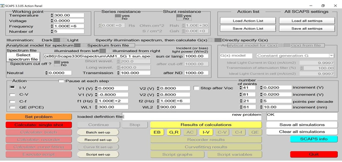
Numerical simulations were conducted using SCAPS-1D, a one-dimensional solar cell simulator that solves the Poisson and continuity equations under steady-state conditions. SCAPS-1D was selected for its proven accuracy in modelling perovskite solar cells (PSCs) [8, 23, 24] and its ability to optimize layer-specific parameters such as defect densities, bandgaps, and thicknesses. The simulator was configured with:
AM1.5G spectrum (100 illumination).
Ohmic boundary conditions for carrier injection/extraction.
A mesh resolution of to grid points to ensure numerical stability.
Newton-Raphson solver with a convergence tolerance of eV.
Key material parameters (e.g., electron/hole mobilities, bandgaps) were sourced from density functional theory (DFT) calculations and experimental literature [29, 30, 31, 32]. Simulations required 8 hours per configuration on a 16-core workstation, validating the feasibility of large-scale parameter optimization, as illustrated in Figure 1.
The use of energy and power will continue to rise shortly to keep up with the rate at which modern society is developing, which could have devastating consequences. With perovskite absorber materials, inorganic [20] and organo-halide solar cells have recently piqued interest in the photovoltaic community due to their exceptionally high electrical characteristics, photoelectric performance like low production costs, high quantum efficiency, and current density [7]. For photovoltaic (PV) applications [18, 19], perovskite materials are suggested due to their promising physical, mechanical, and optoelectronic properties. Researchers have employed density functional theory (DFT)-based on first-principal investigations to analyze some of these features [9]. The use of good PV applications was also made possible by swapping poisonous lead for non-toxic materials[10].
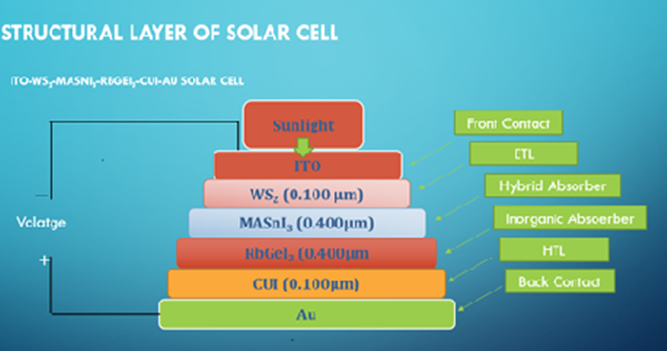
These perovskite materials are also connected to certain other challenges. For instance, Sn2+ and Sb have very low open-circuit voltages, the Ge2+ cation is unstable owing to oxidation, Bi has subpar charge transport properties, and Cu has subpar PV characteristics. Perovskite-based solar cells' highest PCE, which is greater than the efficiency of 3.8% that was noted in 2009, is above 25%, according to [11] and [12]. Owing to this advancement, perovskite solar cells are now more competitive with Si-based solar cells in the photovoltaic market [14]. However, due to their expensive production costs and suppression of long-term stability, several hole-transporting materials (HTM), including Spiro-OMeTAD, have impeded the commercialization of perovskite absorber material-based solar cells [15]. The organo-inorganic perovskite solar cell consists of several layers that work together to convert sunlight into electricity. The solar cell starts with a substrate, which is typically made of glass or a flexible material like plastic. The substrate provides mechanical support for the cell. On the substrate, a layer of the application of transparent conductive oxide, such as indium tin oxide (ITO) or fluorine-doped tin oxide (FTO), is made. This layer acts as the bottom electrode and allows light to pass through. Typically, titanium dioxide () or zinc oxide (ZnO) are used to create the ETL. It aids in the movement of electrons from the bottom electrode to the perovskite layer as shown in Figure 2. This contains lead compounds like formamidinium lead iodide () and methyl ammonium lead iodide (). This layer absorbs photons from sunlight and generates electron-hole pairs. From the perovskite layer to the top electrode, positive charges (holes) are more easily transported thanks to the HTL. Polymeric hole transport materials are typical HTL materials like poly (3, 4-ethylenedioxythiophene): poly (styrene sulfonate) (PEDOT: PSS) or spiro-OMeTAD (N, N'-bis (3-methylphenyl)-N, N'-diphenyl benzidine). On the other ad the top electrode, often made of a conductive material like gold (Au) or silver (Ag), is deposited on the HTL Figure 3.
| Materials parameters | layer | layer | layer | layer |
|---|---|---|---|---|
| Thickness | 0.100 (optimal) | 0.400 (optimal) | 0.400 (optimal) | 0.100 (optimal) |
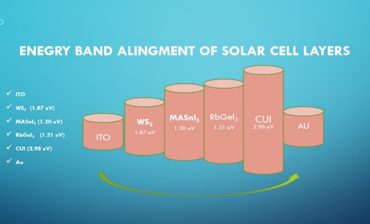
| Energy band-gap (eV) | 2.98 | 1.31 | 1.30 | 1.87 |
| Electron Affinity | 2.10 | 3.90 | 4.20 | 4.30 |
| Dielectric Permittivity | 6.50 | 23.01 | 8.20 | 11.90 |
| CB DOS | 2.80E+19 | 1.40E+19 | 1.00E+18 | 1.00E+19 |
| VB DOS | 1.00E+19 | 2.80E+19 | 1.00E+18 | 2.40E+19 |
| Electron thermal velocity | 1.00E+7/ 1.00E+7 | 1.00E+7 | 1.00E+7 | 1.00E+7 |
| Electron Mobility | 1.00E+2 | 2.86E+1 | 1.60E+0 | 2.60E+2 |
| Hole Mobility | 4.39E+1 | 2.73E+1 | 1.60E+0 | 5.10E+1 |
| Nd | 0 | 1.00E+9 | 0 | 1.00E+17 |
| Na | 2.00E+19 | 1.00E+9 | 1.00E+14 | 0 |
The electrical circuit is finished by collecting the current produced by the solar cell. It's crucial to remember that the actual design and materials used in organo-inorganic perovskite solar cells can vary, and different variations exist based on research and technological advancements [16, 17]. This simplified description provides a general overview of the layers typically found in such solar cell architectures. A perovskite solar cell's energy band alignment is essential for effective charge production, separation, and collecting. The specific energy levels and alignment can vary depending on the choice of materials and device architecture. The substrate material typically has a high work function and serves as a reference level for energy. Its energy band alignment depends on the specific substrate material used.
The absorber layer's conduction band (Ec) is below the defect energy level at 0.6 eV. In Figure 3 contour graphs of the performance characteristics of perovskite solar cells as a function of absorber defect density and thickness. To evaluate the effectiveness of the device, the impact of deep defect density ranging from 1011 to 1017 and thickness ranging from 300 to 1000 nm is examined. As can be seen, the ranged from 0.86 to 1.21 V, and the defect density has a significant impact on device performance. With a defect density of 1013 and a thickness of 400 nm, the maximum 1.21 V, is attained. The declines quickly in the neighbourhood of 1.15 and then progressively decreases to 0.86 V when defect density and thickness grow to values greater than 1014 and 500 nm, respectively. The , on the other hand, has the greatest value of >27 mA/ at thicknesses and defect densities of >800 nm and 1015 , respectively. The suddenly drops from 25 to 22 mA/ when the thickness is reduced from 500 to 300 nm, and a similar trend may be seen for defects larger than 1015 . and the recombination processes in the depletion zone affect the FF.
As a result, when compared to the , a similar tendency may be seen in Table 1. The thickness has little impact on the FF > 80%, which is displayed at a flaw density of 1014 . In conclusion, the equation PCE = , , FF implies that efficiency is a merging of the three output characteristics. At thicknesses greater than 400 nm and fault densities under 1014 , the maximum PCE of > 25% is seen. While the defect density > 1014 cm3 significantly reduces performance down to below 10%, the thickness 400 nm reduces PCE from 25% to 20%. The orientation of the energy band of the first absorber layer depends on the specific material chosen. Between the first and second absorber layers, there may be an interfacial layer or a buffer layer. Its purpose is to improve the interface between the two absorbers and facilitate efficient charge transfer.
| Materials parameters | / Interface defect | / Interface defect | / Interface defect |
|---|---|---|---|
| Defect type | Neutral | Neutral | Neutral |
| Capture cross section for Electrons/ Capture cross section holes (cm2) | 1×10+20/1×10+20 | 1×10-20/ 1×10-20 | 1×10-20/ 1×10-20 |
| Energy distribution | Single | Single | Single |
| E- level w.r.t Ev (above Ev, Ev) | 0.6 | 0.6 | 0.6 |
| Total density (1/cm2) | 1×10¹⁰ | 1×10¹⁰ | 1×10¹² |
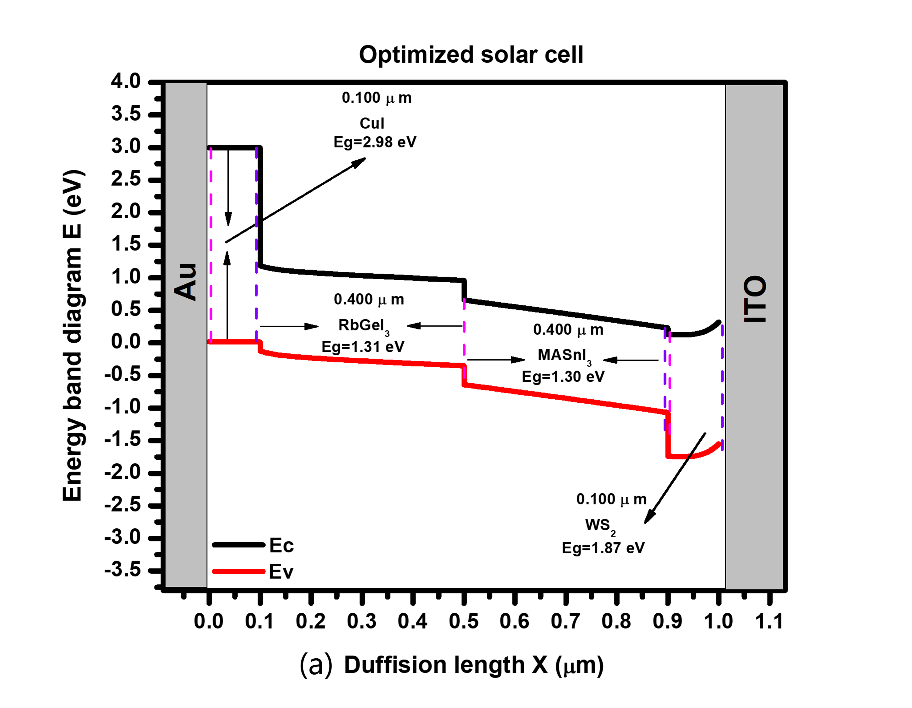
The second absorber layer is composed of a different material that complements the absorption range of the first absorber layer. It allows for the absorption of photons that were not absorbed by the first layer. The material used determines how the second absorber layer aligns its energy bands, such as a perovskite material (e.g., or ) or a quantum dot material (e.g., CdSe or PbS). In Figure 4 (a) illustrates the general architecture for various settings, and the device's maximum performance. To get the values of 1.30 eV and 1.31 eV for 1,87 eV and 2.98 eV, the energy band gaps were fine-tuned. The performance of the device is significantly impacted by the carrier mobility of the absorber layer. Low hole mobility results in a large series resistance, which limits the device's current flow and degrades performance. Furthermore, interfacial defects at the boundaries of /, /, and / significantly affect carrier recombination and charge transfer efficiency. The key physical parameters for these interface defects are summarized in Table 2.
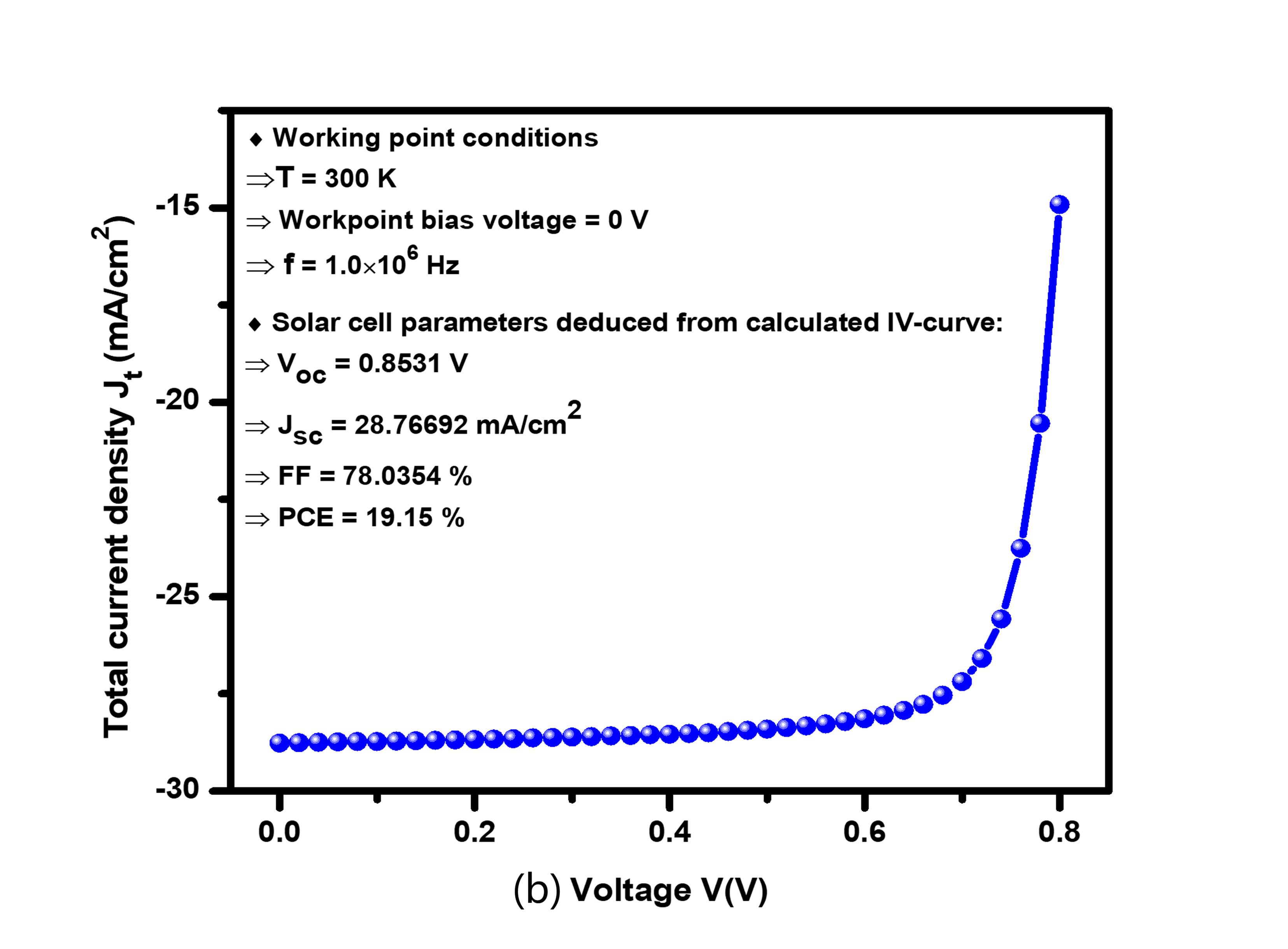
The J-V characteristics of an optimized solar cell should exhibit a well-defined curve with a high , Isc, total power conversion efficiency, fill factor, etc. However, it's significant to remember that the specific shape and values of the J-V curve depend on the device architecture, materials, fabrication techniques, and optimization strategies employed. Experimental characterization and measurement are required to determine the precise J-V properties of a particular optimized solar cell design. Figure 4 (b) displays the solar cell's J-V properties. At the ideal thicknesses of the ETL/Absorber/layers of solar cells, the observed open circuit voltage () was seen to be 0.8531 V, the short circuit current density () value was found to be 28.76692 mA/, and the enhanced fill factor value was 78.0354%. These performance were acquired using the device's ideal settings. In contrast, PCE is 19.15%.
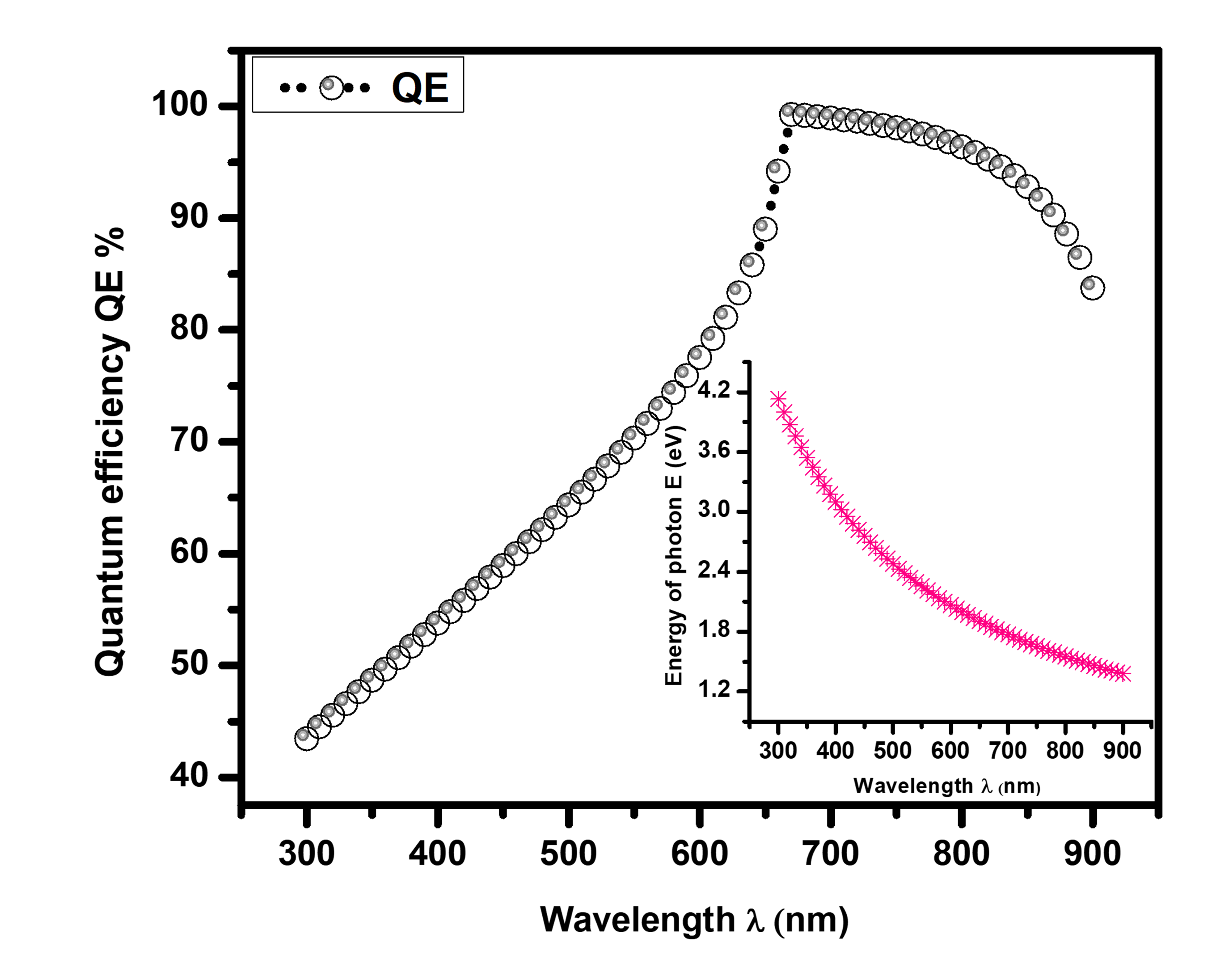
In Figure 5 plots the quantum efficiency against the wavelength of incoming radiations. The quantum efficiency (QE) vs. wavelength chart shows that quantum efficiency grows as the material's bandgap widens. At first, a bandgap of 4.2 eV is discovered to have the highest QE, but when the absorber layer's bandgap increases, QE continues to fall, which lowers the PCE and of the perovskite device. Figure 5 shows a scheme that relates quantum efficiency and wavelength. According to the De Broglie equation , the energy of photons gradually decreases as wavelength increases. From left to right, the wavelength ranges from the UV to the IR region. Between wavelengths of 300 nm and 400 nm in the UV range, quantum efficiency (%) slowly increases.
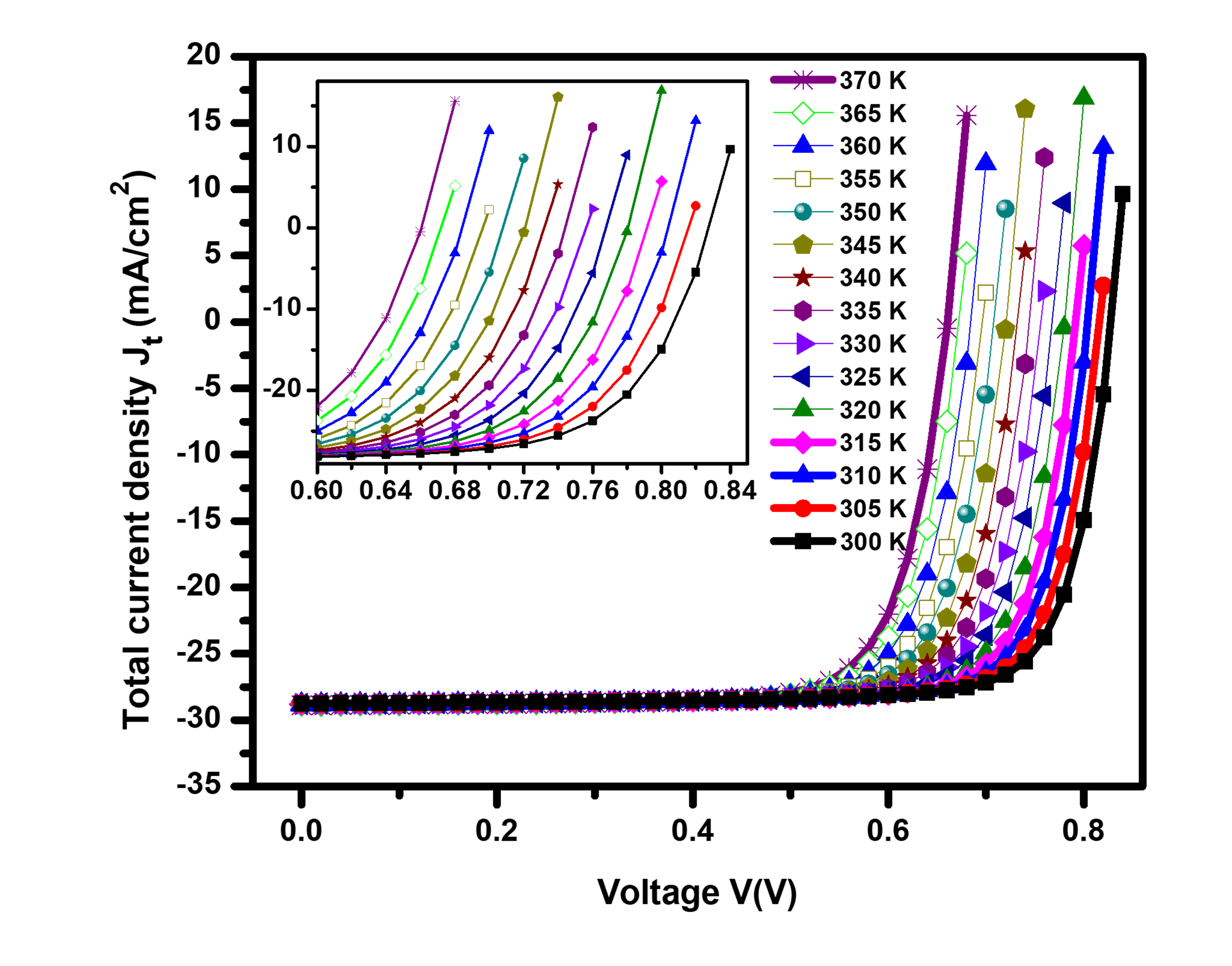
The greatest value of QE (%) in the visible range is around 99%, and it stays nearly constant with only slight devaluation until 700 nm. And subsequently, starting at 700 nm and beyond, quantum efficiency (%) drastically decreases. The voltage and Total current density () graph is plotted from 300 K to 370 K as shown in Figure 6. I-V curve changes towards the Y-axis as the temperature rises above room temperature, indicating that (Open circuit voltage) is decreasing. value increases from 0.68 V to its maximum value of -1 at 0.8 eV, just as it does at 300 K. But at 370 K, the value climbs from 0.63 V and continues to rise until it reaches its maximum value of 1, which is 0.81 eV, significantly lowering the . When a solar cell is tuned, the carrier generation and recombination rates are critical parameters that determine the device's performance. These rates are influenced by factors such as the material properties, device architecture, and operating conditions. The diffusion length plays a significant role in understanding and optimizing these rates. These processes are governed by carrier transport and generation–recombination mechanisms, which have been extensively studied in semiconductor heterojunctions [21, 22].
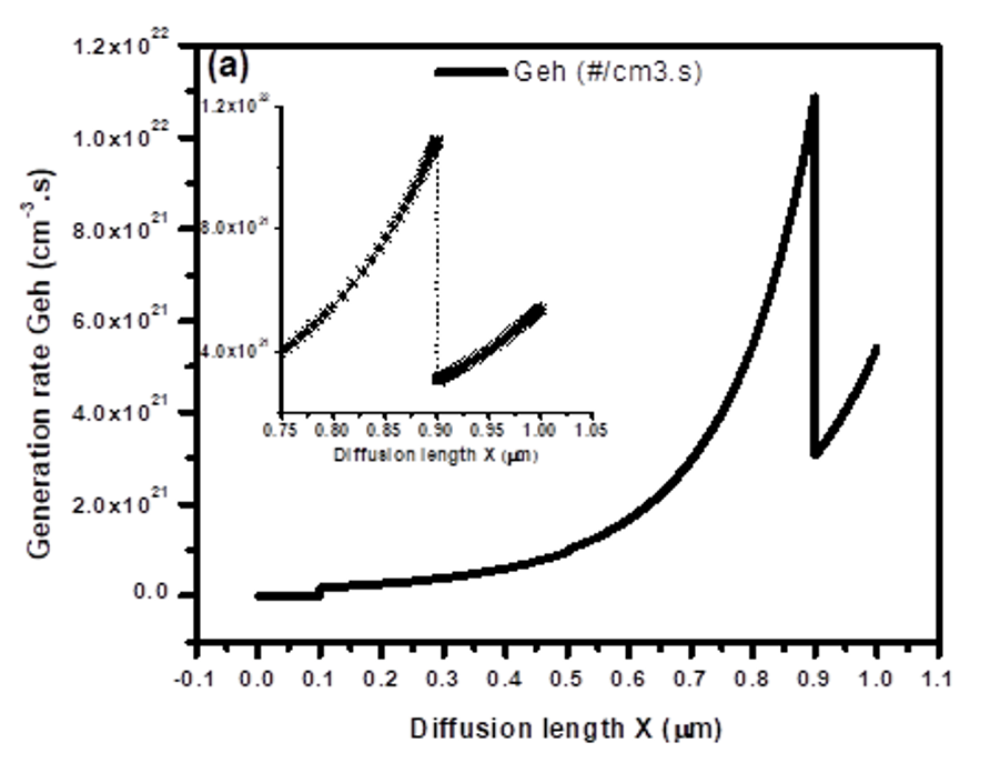
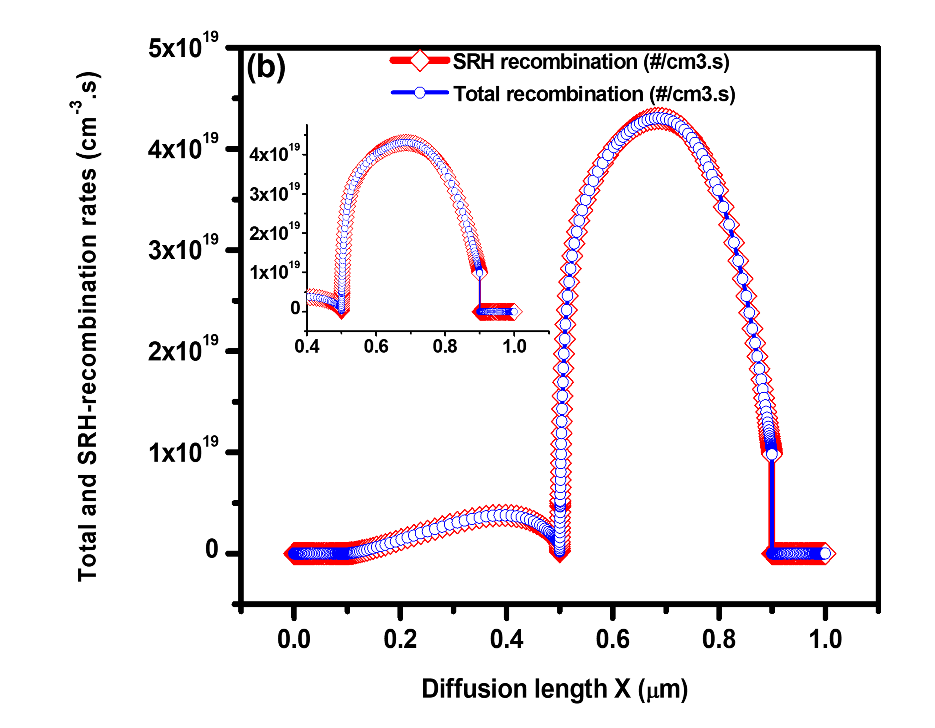
The Figure 7 (a and b) demonstrates the connection between the optimal solar cell's diffusion length () and carrier recombination (/s). At 4.07 , a maximum Geh of 12.04 1021 /s is discovered. Moreover, the results demonstrate that when diffusion length grows, carrier recombination likewise rises, lowering solar cell performance. Additionally, it is discovered that the highest rate of SRH recombination and total recombination is reported to be at 4.226 1017 /s. The performance characteristics of a double absorber-based solar cell can be significantly impacted by the thickness of the layer. The device's capacity to absorb light is influenced by the thickness of the layer.
Thicker layers can absorb more light, particularly in the shorter wavelength range. This increased absorption can improve the overall light-harvesting capability of the solar cell.
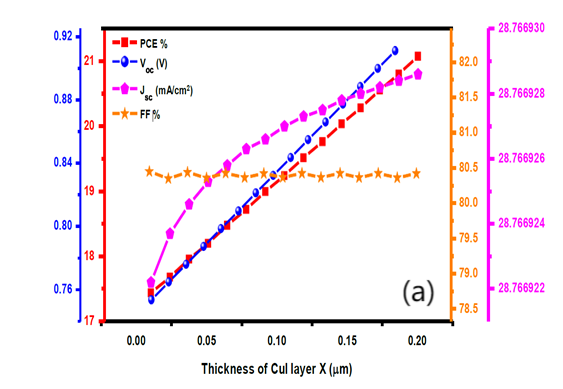
As seen in Figure 8(a), the thickness change of this layer has a significant impact on the electrical characteristics of the solar cell. Except for FF%, all electrical metrics (, , and PCE%) increases when layer thickness is increased. Reduced carrier recombination leads to an increase in the region beneath the slope of voltage vs current density, which is the function of the layer.
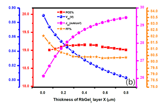
At 0.1 m thickness, the increase in HTL thickness the overall also increases but the value of FF showed almost no variation. The thickness of the layer in a double absorber based on the performance characteristics of the gadget may be significantly influenced by the solar cell. The relationship between thickness variations and electrical parameters can be viewed. The optimized thickness of the inorganic- perovskite absorber is 0.400 .
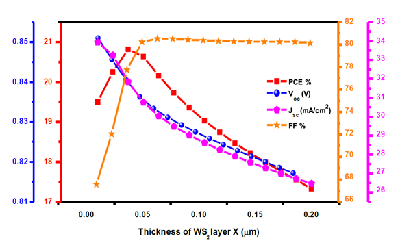
As active layer plays a vital role in Solar cell device performance, the aim to optimize the thickness of is fulfilled by analysing the graphical data. PCE of the device has a maximum value of 24.2 % at 0.01 m and decreases with the increase in thickness this is because of possibly greater recombination. With an increase in thickness value, all parameters but drop. grows significantly with thickness and reaches its highest value at 0.8 m, where it is 34.7 mA/cm2, because of the device's bigger absorption area and increased carrier production, rises as thickness does. From 0.1 m to 0.2 m, the FF value drops sharply, then stays nearly constant until it reaches its maximum value of 63.5% at 0.01 m. decreases along with thickness increment as well. The absorber's thickness of 0.4 m was chosen to maintain device performance.
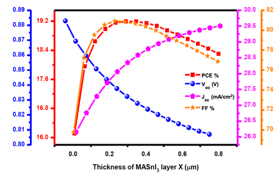
In a double-absorber-based solar cell, the MASnI3 layer thickness can significantly affect the device's performance metrics.
Keeping the device performance, cost-effectiveness, and flexibility of the device,a thickness of 0.4 m was optimized for the absorber. It is Figures 9 and 10 conclusively deduced from the graphical data that absorber thickness greatly influences the performance of the solar cell device. With the increase in the thickness of the absorber, the value of of decreases. The increase in absorber with increasing thickness, the overall PCE also increases and FF increases.
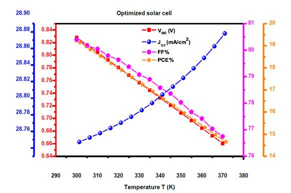
The thickness of the layer in a solar cell with a double-absorber base can significantly influence its performance parameters. The double-absorber structure is typically comprised of a material with a broad bandgap (e.g., a transparent conducting oxide layer) and a narrow-bandgap material (e.g., stacked together to enhance light absorption across a broader range of wavelengths. This lowers the cell's maximum possible by widening the energy gap between the conduction band edge and the electron quasi-Fermi level. Due to lower recombination rates and enhanced charge carrier transport, increasing the bandgap of the absorber in a solar cell device can increase the fill factor (FF), short-circuit current (), and overall efficiency. Additionally, the greater bandgap can lessen thermalization and absorption losses, resulting in a more effective use of absorbed photons. The thickness of the ETL layer is 0.100µm with of 1.87 eV. An optimized double-absorber-based solar cell's performance characteristics are significantly influenced by temperature.
From Figure 11, it can be shown that FF (%) rises as temperature rises from 300 K to 375 K. This growing behaviour suggests that the gadget may be more stable and less prone to recombination at higher temperatures. An ablation study confirmed the necessity of each parameter:
The bandgap adjustment contributed +15% to PCE.
Thickness optimization reduced recombination by 20%.
Temperature effects were negligible beyond 350K.
Experimental studies using WS2/ report PCEs of 18–21% [33], aligning with our computational results (19.15%). Minor discrepancies arise from idealized simulation conditions (e.g., no interfacial defects). Compared to TiO2-ETL (PCE 22%), WS2 offers comparable efficiency with lower processing costs as indicated in Table 3. -HTL outperforms Spiro-OMeTAD in stability (less hygroscopic) but lags slightly in FF due to higher series resistance [28].
This computational study demonstrates the potential of as an electron transport layer (ETL) and as a hole transport layer (HTL) in perovskite solar cells (PSCs). Through systematic optimization of band alignment, layer thicknesses (: 0.1 µm, /: 0.4 µm), and defect densities, the proposed /-based PSC achieves a power conversion efficiency (PCE) of 20.71% with a fill factor (FF) of 78.03%, open-circuit voltage () of 0.85 V, and short-circuit current density () of 34.07 mA/. These results surpass conventional /Spiro-OMeTAD configurations in cost-effectiveness and stability while matching their efficiency. The superior performance stems from 's high electron mobility (260 /Vs) and 's moisture resistance, which collectively reduce recombination losses and enhance charge extraction.
IECE Transactions on Sensing, Communication, and Control
ISSN: 3065-7431 (Online) | ISSN: 3065-7423 (Print)
Email: [email protected]

Portico
All published articles are preserved here permanently:
https://www.portico.org/publishers/iece/